
Printing Plate
MPM leads the world in the development of the Silver Digiplate@ CTP(computer to plate)system.
Based on the printing-related technology cultivated during this development, we are researching and developing new printing plates.
Silver Digiplate® as a trailblazing pioneer in CTP
DTR refers to the diffusion transfer reversal process representing one of the characteristic technologies applied to silver halide photosensitive material. Around this DTR technology axis, we realized higher sensitivity and established technology to form nano particles, which serves as a catalyst to create the silver image suitable for printing. Furthermore, we have developed HHP (hyper-hydrophilic polymer) technology that is used to process the printing plate surface and DWE (Double Wave Effect) technology to optimize the surface roughness so as to obtain hydrophilic printing plate surface. Combining all of these technologies, we finally launched the pioneering. CTP Silver Digiplate®.
Eco-conscious coating-type development process
We are the first manufacturer to introduce the coating-type development process in the market. In this process, development is conducted by applying a minimal amount of chemicals to the plate surface instead of dipping the plate into the chemicals. By this method, the amount of chemical waste was reduced by two-thirds.
Eco-conscious CTP-Thermal Digiplate®(TDP)
We developed the thermal Digiplate® system as an even more eco-friendly CTP. This is a perfectly process-free system and exhausts no chemical and material wastes. This TDP system is a unique integration of the superior printing technology of Silver Digiplate® and the image formation technology of thermal paper. This system releases no waste except the used printing plate itself. Based on this concept, this system was approved to be at the highest level of the E3PA mark by E3PA.
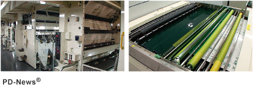
PD-News®, an aluminum-based CTP printing plate for newspaper
Based on organic synthesis background we cultivated in silver halide photography, we have developed novel photopolymer technology with high sensitivity and superior development stability. This technology is applied to PD-News. Unlike traditional thermal CTP plates, PD-News® requires no preheating and pre-washing processes before development. Consequently, this system is highly reliable with less CO2 emissions.
Electronic Materials
We are developing unique products to meet customer needs in the electronic substrate industry by developing technologies we have cultivated in the fields of paper processing and silver halide photosensitive material.
High-density printed circuit board
Flat-screen televisions and mobile terminals are becoming increasingly sophisticated. Therefore, more devices must be mounted in the same space. What enables high-density printed circuit board technology enables the mounting of parts in high density to support this development. Our innovative resist/etching system enabled production of fine circuit patterns.
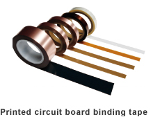
Printed circuit board binding tape
-
Printed circuit boards are manufactured through many processes. In the conventional process, each board is processed one by one and thus production cannot be so efficient. Our printed circuit board binding tape is a solution to this issue. By binding boards with this tape prior to the process, the stability of production and quality can be largely improved. Our tape enabled electroconductive bonding in addition to reliable chemical resistant bonding.. A unique grade that eliminates effort to cut the bonded boards again into pieces, as it automatically releases at the final resist stripping process, is also available.
SF Uitra Fine Conductive Silver Pattern Film
In recent years, demand for drawing hardly visible electroconductive patterns on transparent substrates is increasing, such as electrodes for displays, electromagnetic interference (EMI) shielding, and touch panels. However, it is much more difficult to draw stable conductive patterns whose width is only tens of micrometers over a large area of substrate than one simply expects. We have solved this problem by using DTR technology we had developed for Silver Digiplate®. We are working to launch a variety of products in collaboration with other companies. With Mitsubishi Gas Chemical Company, lnc., we are trying to develop a transparent electromagnetic wave absorber for a dedicated short-range communications (DSRC) system utilized in the intelligent transport system (ITS), which accomplishes the improvement of communication environment and opposite side visibility simultaneously. Also developed is the shock-proof EMI shielding material with high durability. With Fujimori Kogyo Co., Ltd., we have developed EMI shielding film for plasma televisions and are sill making an effort to realize new applications such as transparent electrodes for display, transparent heaters, and touch panels.