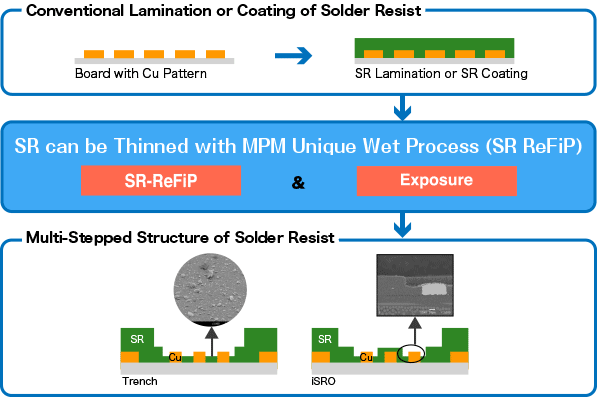
HOME > Electronic materials > Photoresist system, other > New Solder Resist Formation System (SR-ReFiP)

Applications
- Flattened Solder Resist
- Dam Formation for Underfill resin
- Self-Aligned Electrode Pad (Exposure of Electrode Surface in Flip Chip Mounting)
- Any other Multi-Stepped Structure
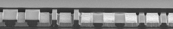
Thinning Uniformity
| Processing Time |
-Thickness | ||||
|---|---|---|---|---|---|
| Max. [µm] |
Min. [µm] |
Ave. [µm] |
STDEV. [µm] |
Rate [µm/sec] |
|
| 10sec | 13.9 | 12.6 | 13.1 | 0.37 | 1.31 |
| 15sec | 18.0 | 16.5 | 17.4 | 0.36 | 1.16 |
| 20sec | 21.2 | 20.1 | 20.7 | 0.33 | 1.04 |
| 25sec | 23.3 | 22.3 | 22.8 | 0.30 | 0.91 |
Panel Size : W510mm×L410mm
Measurement : 20points
- Excellent Uniformity
- High Productivity
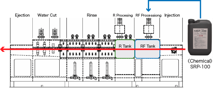
ReFiP Processor
Necessity and Advantage of SR-ReFiP
| Structure | Cu Pad Poor Adhesion |
Ni/Pd/Au Plating Short |
Solder Bridge |
Under Fill Resin Void |
Solder Resist Undercut |
|
|---|---|---|---|---|---|---|
| Conventional | Trench | |||||
| iSRO | ||||||
| SR-ReFiP | Trench | |||||
| iSRO | ||||||
| ETS | ||||||